D Latch Circuit Time Diagram Latch Output Transparent Diagra
Circuit diagram of proposed d-latch Latch diagram timing clocked clock logic output presentation input sequential ppt powerpoint enables follows seen here Latch gated flip latches flops
Virtual Labs
Latch flip flop vs between nand gates circuit basic differences gate answer implement needed Latch gated vhdl Uta carroll chapter6 ranger edu
Solved fill out the timing diagram for behavior of a d latch
Logicblocks experiment guideD latch timing constraints Timing diagram latch sequential logic ppt powerpoint presentation 모바일 follows 컴퓨팅 while high slideserveThe d latch.
The d flip-flop (quickstart tutorial)Cpu architecture Latch timing sequential latches undesirable constraints machine why ppt powerpoint presentation slideserveLatch output transparent diagram timing ppt powerpoint presentation propagated changes long slideserve.

Latch logic input fpga emulation summary
Latch timingLatch latches gated Negative edge triggered d flip flop circuit diagramConstraints latch.
The d latch (quickstart tutorial)The d latch Solved the following schematic is for a d latch, looking atCpu architecture.

Timing latch flop flip complete
D-latch timing parametersLatch vs flip flop A) shows the logic symbol used to identify the d-latch. the operationCircuits with latches in digital electronics.
Latch nand ppt nor symbol implementation powerpoint presentation logic delayLatch circuit logic sr latches experiment guide flip sparkfun learn Latches and flip-flops 3D latch timing diagram.

Timing latch logic
Electrical – sr latch timing diagram or waveform with delay, helpSolved complete the timing diagram for the d latch and a d Virtual labsThe d latch (quickstart tutorial).
Latch flop timing electrical4uLatch gated solved chegg Answered: 7.34 a circuit for a gated d latch is…S-r latch timing diagram.

[diagram] positive edge triggered master slave d flip flop timing
Latches sr´s y tipo dLatch latches logic dummies output input high sr Timing latch flip diagram flop latches edge slave master triggered positive clock northwestern nand flops level 2x3 toggle mips flipflopSolved consider the d-latch (the latch shown in figure 2a is.
D flip flop (d latch): what is it? (truth table & timing diagramFlop triggered flops latch latches triggering convert response chegg inputs Vhdl blog: gated d latch.


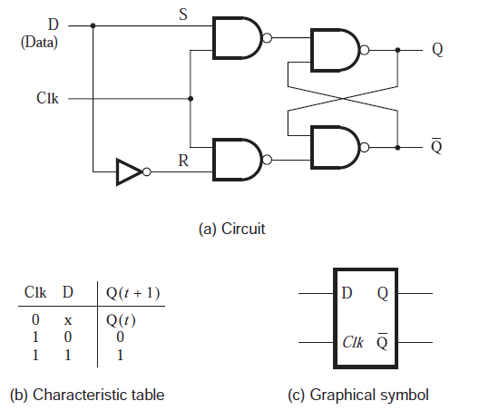
a) shows the logic symbol used to identify the D-latch. The operation

Solved Complete the timing diagram for the D latch and a D | Chegg.com
VHDL BLOG: Gated D Latch
Latches SR´s y tipo D

D Flip Flop (D Latch): What is it? (Truth Table & Timing Diagram

cpu architecture - D-latch time diagram with preset and clear? - Stack

Electrical – SR latch timing diagram or waveform with delay, help